5/7/2020: As part of building CNC machines and my daytime job I have developed a need for better circuit boards for my designs. I started about 15 to 18 years ago and the option I chose was a professional circuit design package (Proteus by lab centre electronics) and wet processing/etching to create the boards. I managed some complicated designs and some of them are still working today although looking a little bit the worse for wear.
Over the last year or so I have been making some new boards and find myself striving for a better product than I had yesteryear. I have sent boards away for professional production and the results have been stunning but usually about 3 weeks away and the shipping etc. costs are heartbreaking. My lab of choice now is http://www.jlcpcb.com and I select the shipping option with prepaid duties, by far the best for me.
My eyes were opened by work being able to mill single sided boards. This set me off on a path of discovery which I will try to document here. I’m still on this journey but I’m getting there.
So, the requirement: I want to be able to produce double sided pcb’s up to 160 by 100mm mixing surface mount and through hole technology. I also want solder resist and ideally silkscreen layers too.
The plan:
- Etch the double sided board
- Use a small cheap mill to drill the holes
- Use the same mill to remove the solder resist from the pads
- Other fancy things like silkscreen printing without the silkscreen kit
Lessons learnt so far:
- Working with solder resist paint is challenging if I’m charitable but I’m pretty much there now
- Getting a cheap Chinese mill up and running is hard work as I learn the various bits of software needed
- Sometimes I wonder if it wouldn’t have been easier to buy a Wegstr or similar for £3500-4000 + extras and a dependency on the manufacturer
- Don’t second guess my chosen path, it’s good learning plus I don’t have that much money
About this time during one of my many hours of surfing I found this Website page which is an excellent read and reflects a lot of my own experiences in pcb production at home. Some of the links are out of date and some components are no longer available e.g. through hole options. The owner of the site referenced above calls it Mike’s Electric Stuff at http://www.electricstuff.co.uk/ and there is lots of information on the home page. Many enjoyable winter hours of reading there.
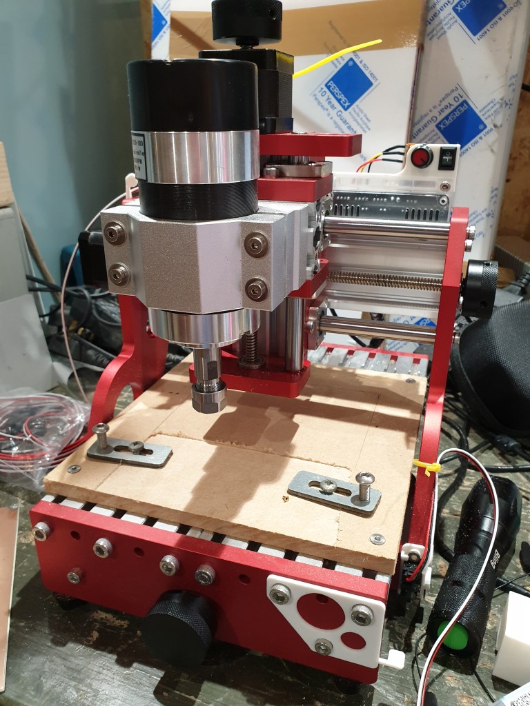
4/8/2020: After some research I decided on a 1419 red mill from China. This ran on grbl so the supporting software was available. A little click here and another there and I was in for a 5 week wait. Never a strong point of mine, waiting. When a friend said there was a similar mill on Facebook a few days later I thought: hmmm, learning opportunity here. Off to Wales to collect the beast and down the learning path we stumbled.
After a while the Chinese one arrived and by now I am slowly getting to grips with the workflow. A few hours spent building it and we were ready to go. There were a couple of mods I made without even fitting the original parts. One was a new upgraded controller running grbl 1.1 and the second was a 400W three phase spindle. Both these upgrades have proven very successful.
Here is the mill after it has completed its first trials. Note I am also experimenting with X and Y end stops for homing only. At the moment the jury is out on this, my gut feel is they won’t be needed.
The second image is my first play with milling a PCB
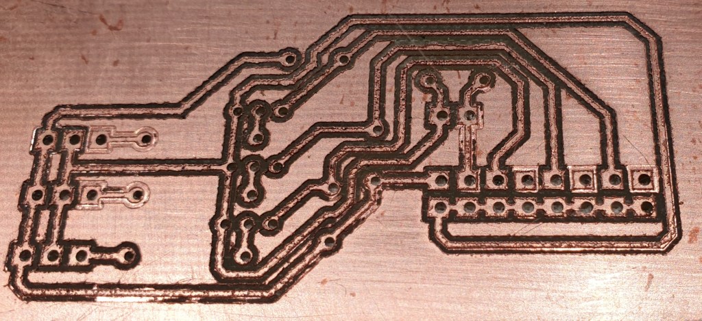
Whilst the above PCB effort may not be terribly good it represents a lot of learning. For example, I used a height map and due to the machine controller going phut between milling and drilling I learnt a lot about realigning work-pieces. You can see all the holes are slightly right of the pads but usable if it were not for all the other issues.
31/8/2020: I’ve been playing some more with this and am looking at modifying my approach slightly. I made a small double sided board where I etched the copper, applied solder resist and then scraped it off the pads using the mill and a diamond drag etching bit. This was successful however I did have some issues around cleaning the pads for tinning afterwards. On my next board I intend to try setting the uv solder resist with a pad mask to see if this is any better. I have made some modifications to my uv box so I hopefully won’t suffer the .5mm slide caused by the conventional lid closing and foam pressure layer. It now goes up and down vertically and currently I just put a weight on it.
10/8/2020: Well, some more boards made and more lessons learnt. The issue I am having is with mixing conventional uv exposure and etching with cnc drilling. Whilst I had read about this somewhen in the distant past I had forgotten about it. The problem is my laser (and inkjet, I tried both) does not print accurately to scale. To put this in perspective over 160mm it can be 2mm out. I have got away with this in the past when hand drilling but the cnc is unforgiving to say the least. I found a work around for the current boards but I’m looking into a more permanent solution…..
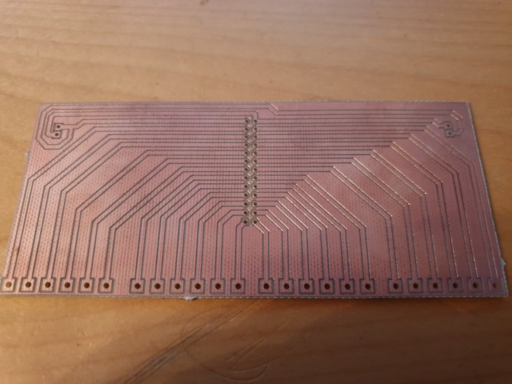
A PCB – the real thing
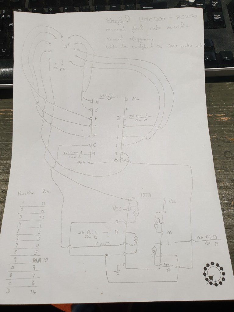
29/9/2020: I have been busy designing a circuit to take the current 11 position (0 to 100%) switch on my Boxford Mill to Gray code. This will mean that for any switch position change only one line into the software will change at a time. The circuit started by understanding how the current version worked which whilst I understand it won’t work moving forward. So, off to the drawing board and I came up with this:
Anyway, create a breadboard circuit and see it in action:
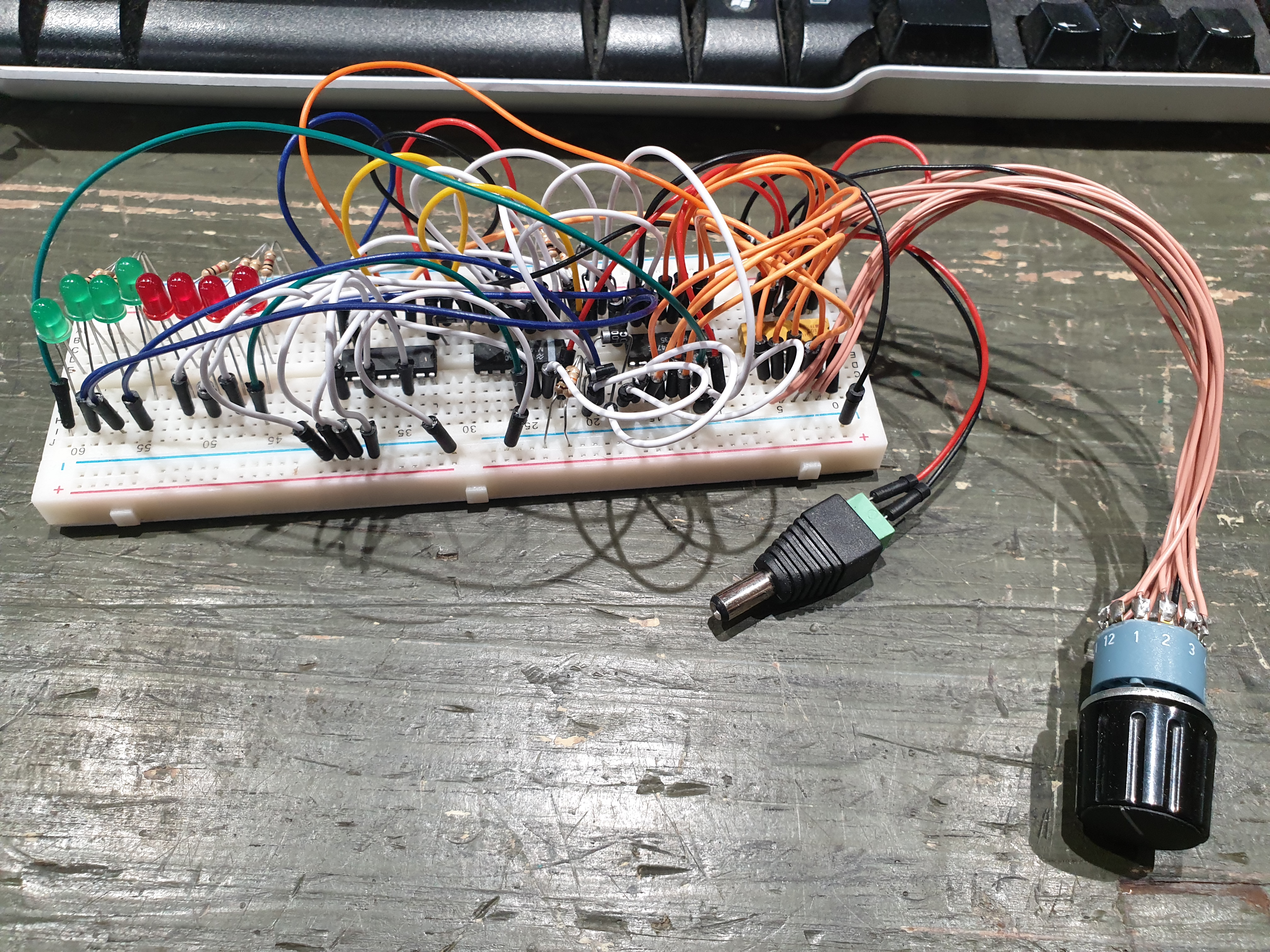

A lot of spaghetti, ok to follow initially and try out some ideas however it pretty soon got a little hard to understand as I tried out more ideas. It was worth it but I had to give up when it turned out it would not all fit in my head. Off to prototype it V2.
Out with the design software, create, think some more, suffer feature creep, repeat several times and a relatively simple idea becomes a monster. Anyway, here is the result of said monster so far.
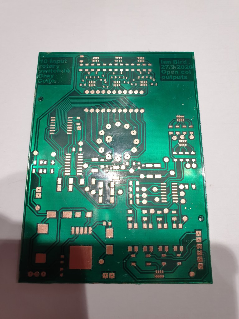

The feature creep manifested itself as four sets of LED’s. There are both binary coded decimal and gray code LEDs, 4 LEDs to indicate the state of the outputs to the interface board (and the fact they are working). By a long shot the cream of the crop is a bar type display at the top with the current position indicated by the off LED. I’m not sure if this is going to be better than a single on LED, we shall see. This last bit was included as when I was using the dial pre this PCB it was annoying not to be able to see the position at a glance.
The next step is to convince the baby red mill to drill the holes for me.
20/10/2020: It turns out as it happens the circuit and the board shown above have a few problems. I have been debugging it but work has been busy so it has been on hold for a while. I did learn the off LED in the bar display was not a good call. I have updated this ready for the next build
Not having the energy to get out into the workshop has meant I have been doing a little more surfing and as it happens thinking about my scaling problem whilst mixing CNC and printing/wet technologies and I have a theory……………
I got inspiration from Peter Liwyj on Hackaday but my main motivation came from ELECTRNOOBS again on Hackaday who used a 3D resin printer as a UV light source in order to expose photosensitive PCB’s. His experiences look very positive so I’m thinking of trying this for myself. The main hiccup at the moment is I don’t have a printer. Roll on Santa this year.
22/10/2020: I did a little more debugging on the circuit above last night and found I had made a silly copy and paste error in the circuit design. I have rectified this now but really need to remake the pcb. This will give me the opportunity to try out the scaling function of the software print function to get around the inaccuracies of the printer. We’ll see soon
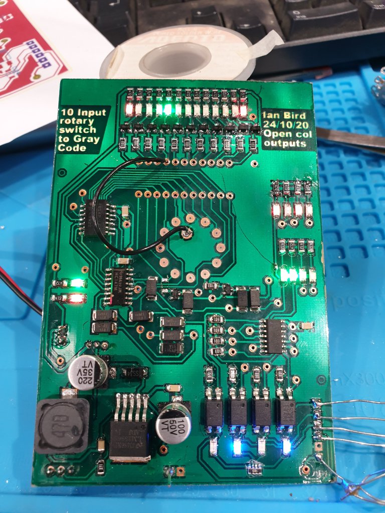
30/10/2020: I have remade the PCB and it works a lot better now. Unfortunately it’s not perfect yet, the BCD is outputting correctly however the Gray code indication is stuck so a little more debugging needed. I have also hit a problem which will necessitate another PCB iteration. The problem is the standard output goes from 6 to 14 (decimal) with no input being 15. This no input state means I cannot easily impose a logic state being equal to binary 5 because sending a zero does not pull the line low if it is high from another source. The answer is to invert the outputs straight out of the encoder which now means no input equals 0 and the standard inputs go from 1 to 9. The final value of 0 will be all low from the encoder allowing me to superimpose the binary value onto the outputs and hey presto. This is now plan C I think but we are getting there for sure. Here is a photo of the populated board from plan B. The scruffy soldered resistors in the bottom right show the open collector output LEDs working. Normally this is provided by the pull ups on the break out board. Interestingly all the components you see on the board are the same ones that were soldered onto the first version. Not a bad recovery technique!
More soon
